Signal integrity is a real issue with dimm modules. It’s the same reason you don’t see modular VRAM on GPUs. If the ram needs to behave like VRAM, it needs to run at VRAM speeds.
Apparently AMD couldn’t make the signal integrity work out with socketed RAM. (source: LTT video with Framework CEO)
IMHO: Up until now, using soldered RAM was lazy and cheap bullshit. But I do think we are at the limit of what’s reasonable to do over socketed RAM. In high performance datacenter applications, socketed RAM is on it’s way out (see: MI300A, Grace-{Hopper,Blackwell},Xeon Max), with onboard memory gaining ground. I think we’ll see the same trend on consumer stuff as well. Requirements on memory bandwidth and latency are going up with recent trends like powerful integrated graphics and AI-slop, and socketed RAM simply won’t work.
It’s sad, but in a few generations I think only the lower end consumer CPUs will be possible to use with socketed RAM. I’m betting the high performance consumer CPUs will require not only soldered, but on-board RAM.
I definitely wouldn’t mind soldered RAM if there’s still an expansion socket. Solder in at least a reasonable minimum (16G?) and not the cheap stuff but memory that can actually use the signal integrity advantage, I may want more RAM but it’s fine if it’s a bit slower. You can leave out the DIMM slot but then have at least one PCIe x16 expansion slot. A free one, one in addition to the GPU slot. PCIe latency isn’t stellar but on the upside, expansion boards would come with their own memory controllers, and push come to shove you can configure the faster RAM as cache / the expansion RAM as swap.
Heck, throw the memory into the CPU package. It’s not like there’s ever a situation where you don’t need RAM.
All your RAM needs to be the same speed unless you want to open up a rabbit hole. All attempts at that thus far have kinda flopped. You can make very good use of such systems, but I’ve only seen it succeed with software specifically tailored for that use case (say databases or simulations).
The way I see it, RAM in the future will be on package and non-expandable. CXL might get some traction, but naah.
Couldn’t you just treat the socketed ram like another layer of memory effectively meaning that L1-3 are on the CPU “L4” would be soldered RAM and then L5 would be extra socketed RAM? Alternatively couldn’t you just treat it like really fast swap?
Wrote a longer reply to someone else, but briefly, yes, you are correct. Kinda.
Caches won’t help with bandwidth-bound compute (read: ”AI”) it the streamed dataset is significantly larger than the cache. A cache will only speed up repeated access to a limited set of data.
Using it as cache would reduce total capacity as cache implies coherence, and treating it as ordinary swap would mean copying to main memory before you access it which is silly when you can access it directly. That is you’d want to write a couple of lines of kernel code to use it effectively but it’s nowhere close to rocket science. Nowhere near as complicated as making proper use of NUMA architectures.
The cache hierarchy has flopped? People aren’t using swap?
NUMA also hasn’t flopped, it’s just that most systems aren’t multi socket, or clusters. Different memory speeds connected to the same CPU is not ideal and you don’t build a system like that but among upgraded systems that’s not rare at all and software-wise worst thing that’ll happen is you get the lower memory speed. Which you’d get anyway if you only had socketed RAM.
Yeah, the cache hierarchy is behaving kinda wonky lately. Many AI workloads (and that’s what’s driving development lately) are constrained by bandwidth, and cache will only help you with a part of that. Cache will help with repeated access, not as much with streaming access to datasets much larger than the cache (i.e. many current AI models).
Intel already tried selling CPUs with both on-package HBM and slotted DDR-RAM. No one wanted it, as the performance gains of the expensive HBM evaporated completely as soon as you touched memory out-of-package. (Assuming workloads bound by memory bandwidth, which currently dominate the compute market)
To get good performance out of that, you may need to explicitly code the memory transfers to enable prefetch (preferably asynchronous) from the slower memory into the faster, á la classic GPU programming. YMMW.
I wasn’t really thinking of HPC but my next gaming rig, TBH. The OS can move often accessed pages into faster RAM just as it can move busy threads to faster cores, gaining you some fps a second or two after alt-tabbing back to the game after messing around with firefox. If it wasn’t for memory controllers generally driving channels all at the same speed that could already be a thing right now. It definitely already was a thing back in the days of swapping out to spinning platters.
Not sure about HBM in CPUs in general but with packaging advancement any in-package stuff is only going to become cheaper, HBM, pedestrian bandwidth, doesn’t matter.
In systems where memory speed are mismatched, the system runs at the slowest module’s speed. So literally making the soldered, faster memory slower. Why even have soldered memory at that point?
I’d assume the soldered memory to have a dedicated memory controller. There’s also no hard requirement that a single controller can’t drive different channels at different speeds. The only hard requirement is that one channel needs to run at one speed.
…and the whole thing becomes completely irrelevant when we’re talking about PCIe expansion cards the memory controller doesn’t care.
I get it but imagine the GPU style markup when all mobos have a set amount of RAM. You’ll have two identical boards except for $30 worth of memory with a price spread of $200+. Not fun.
I don’t think you are wrong, but I don’t think you go far enough. In a few generations, the only option for top performance will be a SoC. You’ll get to pick which SoC you want and what box you want to put it in.
System in a Package (SiP) at least. Might not be efficient to etch the logic and that much memory onto the same silicon die, as the latest and greatest TSMC node will likely be much more expensive per square mm than the cutting edge memory production node from Samsung or whatever foundry where the memory is being made.
But with advanced packaging going the way it’s been over the last decade or so, it’s going to be hard to compete with the latency/throughout of an in-package interposer. You can only do so much with the vias/pathways on a printed circuit board.


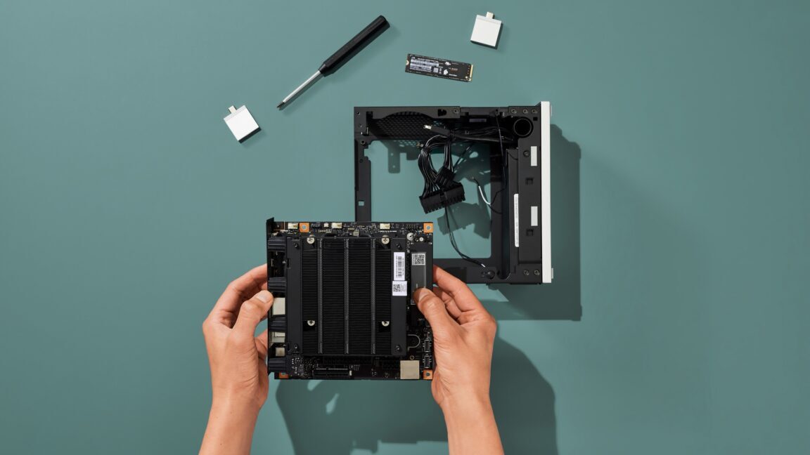
Soldered on ram and GPU. Strange for Framework.
Ye the soldered ram is for sure making me doubt framework now.
Apparently AMD wasn’t able to make socketed RAM work, timings aren’t viable. So Framework has the choice of doing it this way or not doing it at all.
In that case, not at all is the right choice until AMD can figure out that frankly brain dead easy thing.
Signal integrity is a real issue with dimm modules. It’s the same reason you don’t see modular VRAM on GPUs. If the ram needs to behave like VRAM, it needs to run at VRAM speeds.
Apparently AMD couldn’t make the signal integrity work out with socketed RAM. (source: LTT video with Framework CEO)
IMHO: Up until now, using soldered RAM was lazy and cheap bullshit. But I do think we are at the limit of what’s reasonable to do over socketed RAM. In high performance datacenter applications, socketed RAM is on it’s way out (see: MI300A, Grace-{Hopper,Blackwell},Xeon Max), with onboard memory gaining ground. I think we’ll see the same trend on consumer stuff as well. Requirements on memory bandwidth and latency are going up with recent trends like powerful integrated graphics and AI-slop, and socketed RAM simply won’t work.
It’s sad, but in a few generations I think only the lower end consumer CPUs will be possible to use with socketed RAM. I’m betting the high performance consumer CPUs will require not only soldered, but on-board RAM.
Finally, some Grace Hopper to make everyone happy: https://youtube.com/watch?v=gYqF6-h9Cvg
I definitely wouldn’t mind soldered RAM if there’s still an expansion socket. Solder in at least a reasonable minimum (16G?) and not the cheap stuff but memory that can actually use the signal integrity advantage, I may want more RAM but it’s fine if it’s a bit slower. You can leave out the DIMM slot but then have at least one PCIe x16 expansion slot. A free one, one in addition to the GPU slot. PCIe latency isn’t stellar but on the upside, expansion boards would come with their own memory controllers, and push come to shove you can configure the faster RAM as cache / the expansion RAM as swap.
Heck, throw the memory into the CPU package. It’s not like there’s ever a situation where you don’t need RAM.
All your RAM needs to be the same speed unless you want to open up a rabbit hole. All attempts at that thus far have kinda flopped. You can make very good use of such systems, but I’ve only seen it succeed with software specifically tailored for that use case (say databases or simulations).
The way I see it, RAM in the future will be on package and non-expandable. CXL might get some traction, but naah.
Couldn’t you just treat the socketed ram like another layer of memory effectively meaning that L1-3 are on the CPU “L4” would be soldered RAM and then L5 would be extra socketed RAM? Alternatively couldn’t you just treat it like really fast swap?
Wrote a longer reply to someone else, but briefly, yes, you are correct. Kinda.
Caches won’t help with bandwidth-bound compute (read: ”AI”) it the streamed dataset is significantly larger than the cache. A cache will only speed up repeated access to a limited set of data.
Could it work?
Yes, but it would require:
Right now, the easiest solution for fast, high-bandwidth RAM is just to solder all of it.
Using it as cache would reduce total capacity as cache implies coherence, and treating it as ordinary swap would mean copying to main memory before you access it which is silly when you can access it directly. That is you’d want to write a couple of lines of kernel code to use it effectively but it’s nowhere close to rocket science. Nowhere near as complicated as making proper use of NUMA architectures.
The cache hierarchy has flopped? People aren’t using swap?
NUMA also hasn’t flopped, it’s just that most systems aren’t multi socket, or clusters. Different memory speeds connected to the same CPU is not ideal and you don’t build a system like that but among upgraded systems that’s not rare at all and software-wise worst thing that’ll happen is you get the lower memory speed. Which you’d get anyway if you only had socketed RAM.
Yeah, the cache hierarchy is behaving kinda wonky lately. Many AI workloads (and that’s what’s driving development lately) are constrained by bandwidth, and cache will only help you with a part of that. Cache will help with repeated access, not as much with streaming access to datasets much larger than the cache (i.e. many current AI models).
Intel already tried selling CPUs with both on-package HBM and slotted DDR-RAM. No one wanted it, as the performance gains of the expensive HBM evaporated completely as soon as you touched memory out-of-package. (Assuming workloads bound by memory bandwidth, which currently dominate the compute market)
To get good performance out of that, you may need to explicitly code the memory transfers to enable prefetch (preferably asynchronous) from the slower memory into the faster, á la classic GPU programming. YMMW.
I wasn’t really thinking of HPC but my next gaming rig, TBH. The OS can move often accessed pages into faster RAM just as it can move busy threads to faster cores, gaining you some fps a second or two after alt-tabbing back to the game after messing around with firefox. If it wasn’t for memory controllers generally driving channels all at the same speed that could already be a thing right now. It definitely already was a thing back in the days of swapping out to spinning platters.
Not sure about HBM in CPUs in general but with packaging advancement any in-package stuff is only going to become cheaper, HBM, pedestrian bandwidth, doesn’t matter.
In systems where memory speed are mismatched, the system runs at the slowest module’s speed. So literally making the soldered, faster memory slower. Why even have soldered memory at that point?
I’d assume the soldered memory to have a dedicated memory controller. There’s also no hard requirement that a single controller can’t drive different channels at different speeds. The only hard requirement is that one channel needs to run at one speed.
…and the whole thing becomes completely irrelevant when we’re talking about PCIe expansion cards the memory controller doesn’t care.
Honestly I upgrade every few years and isually have to purchase a new mobo anyhow. I do think this could lead to less options for mobos though.
I get it but imagine the GPU style markup when all mobos have a set amount of RAM. You’ll have two identical boards except for $30 worth of memory with a price spread of $200+. Not fun.
I don’t think you are wrong, but I don’t think you go far enough. In a few generations, the only option for top performance will be a SoC. You’ll get to pick which SoC you want and what box you want to put it in.
System in a Package (SiP) at least. Might not be efficient to etch the logic and that much memory onto the same silicon die, as the latest and greatest TSMC node will likely be much more expensive per square mm than the cutting edge memory production node from Samsung or whatever foundry where the memory is being made.
But with advanced packaging going the way it’s been over the last decade or so, it’s going to be hard to compete with the latency/throughout of an in-package interposer. You can only do so much with the vias/pathways on a printed circuit board.
You are correct, I’m referring to on package. Need more coffee.